Handbook Advanced Plasma Processing (19 results)
Search filters
Product Type
- All Product Types
- Books (19)
- Magazines & Periodicals (No further results match this refinement)
- Comics (No further results match this refinement)
- Sheet Music (No further results match this refinement)
- Art, Prints & Posters (No further results match this refinement)
- Photographs (No further results match this refinement)
- Maps (No further results match this refinement)
- Manuscripts & Paper Collectibles (No further results match this refinement)
Condition Learn more
- New (16)
- As New, Fine or Near Fine (3)
- Very Good or Good (No further results match this refinement)
- Fair or Poor (No further results match this refinement)
- As Described (No further results match this refinement)
Binding
Collectible Attributes
- First Edition (No further results match this refinement)
- Signed (No further results match this refinement)
- Dust Jacket (No further results match this refinement)
- Seller-Supplied Images (12)
- Not Print on Demand (17)
Language (1)
Price
- Any Price
- Under � 20 (No further results match this refinement)
- � 20 to � 40 (No further results match this refinement)
- Over � 40
Free Shipping
- Free Shipping to U.S.A. (No further results match this refinement)
Seller Location
Seller Rating
-
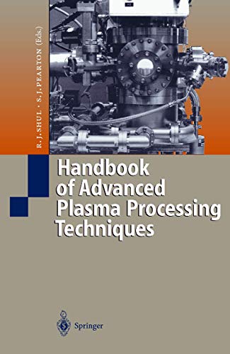
Handbook of Advanced Plasma Processing Techniques
Published by Springer Berlin Heidelberg, 2000
ISBN 10: 3540667725 ISBN 13: 9783540667728
Language: English
Seller: Buchpark, Trebbin, Germany
Condition: Sehr gut. Zustand: Sehr gut | Sprache: Englisch | Produktart: B�cher.
-
Condition: new.
-
hardcover. Condition: New. In shrink wrap. Looks like an interesting title!
-
Handbook of Advanced Plasma Processing Techniques
Seller: Ria Christie Collections, Uxbridge, United Kingdom
Condition: New. In.
-
Handbook of Advanced Plasma Processing Techniques
Seller: Ria Christie Collections, Uxbridge, United Kingdom
Condition: New. In.
-
Handbook of Advanced Plasma Processing Techniques
Seller: GreatBookPricesUK, Woodford Green, United Kingdom
Condition: New.
-
Condition: New.
-
Condition: As New. Unread book in perfect condition.
-
Handbook of Advanced Plasma Processing Techniques
Seller: GreatBookPricesUK, Woodford Green, United Kingdom
Condition: As New. Unread book in perfect condition.
-
Handbook of Advanced Plasma Processing Techniques
Published by Springer Berlin Heidelberg, 2000
ISBN 10: 3540667725 ISBN 13: 9783540667728
Language: English
Seller: moluna, Greven, Germany
Gebunden. Condition: New.
-
Handbook of Advanced Plasma Processing Techniques
Published by Springer Berlin Heidelberg, 2012
ISBN 10: 3642630960 ISBN 13: 9783642630965
Language: English
Seller: moluna, Greven, Germany
Condition: New.
-
Handbook of Advanced Plasma Processing Techniques
Published by Springer Berlin Heidelberg, Springer Berlin Heidelberg Aug 2000, 2000
ISBN 10: 3540667725 ISBN 13: 9783540667728
Language: English
Seller: buchversandmimpf2000, Emtmannsberg, BAYE, Germany
Buch. Condition: Neu. Neuware -Pattern transfer by dry etching and plasma-enhanced chemical vapor de position are two of the cornerstone techniques for modern integrated cir cuit fabrication. The success of these methods has also sparked interest in their application to other techniques, such as surface-micromachined sen sors, read/write heads for data storage and magnetic random access memory (MRAM). The extremely complex chemistry and physics of plasmas and their interactions with the exposed surfaces of semiconductors and other materi als is often overlooked at the manufacturing stage. In this case, the process is optimized by an informed 'trial-and-error' approach which relies heavily on design-of-experiment techniques and the intuition of the process engineer. The need for regular cleaning of plasma reactors to remove built-up reaction or precursor gas products adds an extra degree of complexity because the interaction of the reactive species in the plasma with the reactor walls can also have a strong effect on the number of these species available for etching or deposition. Since the microelectronics industry depends on having high process yields at each step of the fabrication process, it is imperative that a full understanding of plasma etching and deposition techniques be achieved.Springer Verlag GmbH, Tiergartenstr. 17, 69121 Heidelberg 672 pp. Englisch.
-
Handbook of Advanced Plasma Processing Techniques
Published by Springer Berlin Heidelberg, Springer Berlin Heidelberg Nov 2012, 2012
ISBN 10: 3642630960 ISBN 13: 9783642630965
Language: English
Seller: buchversandmimpf2000, Emtmannsberg, BAYE, Germany
Taschenbuch. Condition: Neu. Neuware -Pattern transfer by dry etching and plasma-enhanced chemical vapor de position are two of the cornerstone techniques for modern integrated cir cuit fabrication. The success of these methods has also sparked interest in their application to other techniques, such as surface-micromachined sen sors, read/write heads for data storage and magnetic random access memory (MRAM). The extremely complex chemistry and physics of plasmas and their interactions with the exposed surfaces of semiconductors and other materi als is often overlooked at the manufacturing stage. In this case, the process is optimized by an informed 'trial-and-error' approach which relies heavily on design-of-experiment techniques and the intuition of the process engineer. The need for regular cleaning of plasma reactors to remove built-up reaction or precursor gas products adds an extra degree of complexity because the interaction of the reactive species in the plasma with the reactor walls can also have a strong effect on the number of these species available for etching or deposition. Since the microelectronics industry depends on having high process yields at each step of the fabrication process, it is imperative that a full understanding of plasma etching and deposition techniques be achieved.Springer Verlag GmbH, Tiergartenstr. 17, 69121 Heidelberg 672 pp. Englisch.
-
Handbook of Advanced Plasma Processing Techniques
Published by Springer Berlin Heidelberg, Springer Berlin Heidelberg, 2012
ISBN 10: 3642630960 ISBN 13: 9783642630965
Language: English
Seller: AHA-BUCH GmbH, Einbeck, Germany
Taschenbuch. Condition: Neu. Druck auf Anfrage Neuware - Printed after ordering - Pattern transfer by dry etching and plasma-enhanced chemical vapor de position are two of the cornerstone techniques for modern integrated cir cuit fabrication. The success of these methods has also sparked interest in their application to other techniques, such as surface-micromachined sen sors, read/write heads for data storage and magnetic random access memory (MRAM). The extremely complex chemistry and physics of plasmas and their interactions with the exposed surfaces of semiconductors and other materi als is often overlooked at the manufacturing stage. In this case, the process is optimized by an informed 'trial-and-error' approach which relies heavily on design-of-experiment techniques and the intuition of the process engineer. The need for regular cleaning of plasma reactors to remove built-up reaction or precursor gas products adds an extra degree of complexity because the interaction of the reactive species in the plasma with the reactor walls can also have a strong effect on the number of these species available for etching or deposition. Since the microelectronics industry depends on having high process yields at each step of the fabrication process, it is imperative that a full understanding of plasma etching and deposition techniques be achieved.
-
Handbook of Advanced Plasma Processing Techniques
Published by Springer Berlin Heidelberg, Springer Berlin Heidelberg, 2000
ISBN 10: 3540667725 ISBN 13: 9783540667728
Language: English
Seller: AHA-BUCH GmbH, Einbeck, Germany
Buch. Condition: Neu. Druck auf Anfrage Neuware - Printed after ordering - Pattern transfer by dry etching and plasma-enhanced chemical vapor de position are two of the cornerstone techniques for modern integrated cir cuit fabrication. The success of these methods has also sparked interest in their application to other techniques, such as surface-micromachined sen sors, read/write heads for data storage and magnetic random access memory (MRAM). The extremely complex chemistry and physics of plasmas and their interactions with the exposed surfaces of semiconductors and other materi als is often overlooked at the manufacturing stage. In this case, the process is optimized by an informed 'trial-and-error' approach which relies heavily on design-of-experiment techniques and the intuition of the process engineer. The need for regular cleaning of plasma reactors to remove built-up reaction or precursor gas products adds an extra degree of complexity because the interaction of the reactive species in the plasma with the reactor walls can also have a strong effect on the number of these species available for etching or deposition. Since the microelectronics industry depends on having high process yields at each step of the fabrication process, it is imperative that a full understanding of plasma etching and deposition techniques be achieved.
-
Hardcover. Condition: Brand New. 653 pages. 9.75x6.75x1.00 inches. In Stock.
-
Paperback. Condition: Brand New. reprint edition. 672 pages. 9.25x6.10x1.93 inches. In Stock.
-
Handbook of Advanced Plasma Processing Techniques
Published by Springer Berlin Heidelberg, Springer Berlin Heidelberg Aug 2000, 2000
ISBN 10: 3540667725 ISBN 13: 9783540667728
Language: English
Seller: BuchWeltWeit Ludwig Meier e.K., Bergisch Gladbach, Germany
Buch. Condition: Neu. This item is printed on demand - it takes 3-4 days longer - Neuware -Pattern transfer by dry etching and plasma-enhanced chemical vapor de position are two of the cornerstone techniques for modern integrated cir cuit fabrication. The success of these methods has also sparked interest in their application to other techniques, such as surface-micromachined sen sors, read/write heads for data storage and magnetic random access memory (MRAM). The extremely complex chemistry and physics of plasmas and their interactions with the exposed surfaces of semiconductors and other materi als is often overlooked at the manufacturing stage. In this case, the process is optimized by an informed 'trial-and-error' approach which relies heavily on design-of-experiment techniques and the intuition of the process engineer. The need for regular cleaning of plasma reactors to remove built-up reaction or precursor gas products adds an extra degree of complexity because the interaction of the reactive species in the plasma with the reactor walls can also have a strong effect on the number of these species available for etching or deposition. Since the microelectronics industry depends on having high process yields at each step of the fabrication process, it is imperative that a full understanding of plasma etching and deposition techniques be achieved. 672 pp. Englisch.
-
Handbook of Advanced Plasma Processing Techniques
Published by Springer Berlin Heidelberg, Springer Berlin Heidelberg Nov 2012, 2012
ISBN 10: 3642630960 ISBN 13: 9783642630965
Language: English
Seller: BuchWeltWeit Ludwig Meier e.K., Bergisch Gladbach, Germany
Taschenbuch. Condition: Neu. This item is printed on demand - it takes 3-4 days longer - Neuware -Pattern transfer by dry etching and plasma-enhanced chemical vapor de position are two of the cornerstone techniques for modern integrated cir cuit fabrication. The success of these methods has also sparked interest in their application to other techniques, such as surface-micromachined sen sors, read/write heads for data storage and magnetic random access memory (MRAM). The extremely complex chemistry and physics of plasmas and their interactions with the exposed surfaces of semiconductors and other materi als is often overlooked at the manufacturing stage. In this case, the process is optimized by an informed 'trial-and-error' approach which relies heavily on design-of-experiment techniques and the intuition of the process engineer. The need for regular cleaning of plasma reactors to remove built-up reaction or precursor gas products adds an extra degree of complexity because the interaction of the reactive species in the plasma with the reactor walls can also have a strong effect on the number of these species available for etching or deposition. Since the microelectronics industry depends on having high process yields at each step of the fabrication process, it is imperative that a full understanding of plasma etching and deposition techniques be achieved. 672 pp. Englisch.


